- 您现在的位置:买卖IC网 > Sheet目录3882 > PIC16F87T-E/ML (Microchip Technology)IC MCU FLASH 4KX14 EEPROM 28QFN
196
8008H–AVR–04/11
ATtiny48/88
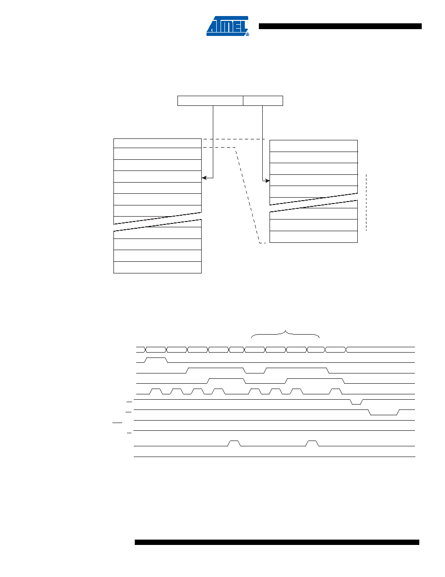
Flash page addressing is illustrated in Figure 21-2, below. Symbols used are described in Table
.
Figure 21-2. Addressing the Flash Which is Organized in Pages
Flash programming waveforms are illustrated in Figure 21-3, where XX means “don’t care” and
letters refer to the programming steps described earlier.
Figure 21-3. Programming the Flash Waveforms
21.2.5
Programming the EEPROM
The EEPROM is organized in pages, see Table 21-2 on page 191. When programming the
EEPROM, the program data is latched into a page buffer. This allows one page of data to be
PROGRAM MEMORY
WORD ADDRESS
WITHIN A PAGE
PAGE ADDRESS
WITHIN THE FLASH
INSTRUCTION WORD
PAGE
PCWORD[PAGEMSB:0]:
00
01
02
PAGEEND
PAGE
PCWORD
PCPAGE
PCMSB
PAGEMSB
PROGRAM
COUNTER
RDY/BSY
WR
OE
RESET +12V
PAGEL
BS2
0x10
ADDR. LOW
ADDR. HIGH
DATA
DATA LOW
DATA HIGH
ADDR. LOW
DATA LOW
DATA HIGH
XA1
XA0
BS1
CLKI
XX
AB
CD
E
B
C
D
E
G
H
F
发布紧急采购,3分钟左右您将得到回复。
相关PDF资料
PIC16F87-E/ML
IC MCU FLASH 4KX14 EEPROM 28QFN
PIC18LF4320-I/ML
IC MCU FLASH 4KX16 EEPROM 44QFN
PIC16F77T-I/PTG
IC MCU FLASH 8KX14 W/AD 44TQFP
PIC16LF1933-I/SO
IC PIC MCU FLASH 4K 28-SOIC
PIC16C54C-20I/SO
IC MCU OTP 512X12 18SOIC
PIC16LF726-I/SO
IC PIC MCU FLASH 8K 1.8V 28-SOIC
PIC12CE673-10/P
IC MCU OTP 1KX14 A/D&EE 8DIP
PIC16F726-I/SO
IC PIC MCU FLASH 8KX14 28-SOIC
相关代理商/技术参数
PIC16F87T-E/SO
功能描述:8位微控制器 -MCU 20MHz 4K Flash RoHS:否 制造商:Silicon Labs 核心:8051 处理器系列:C8051F39x 数据总线宽度:8 bit 最大时钟频率:50 MHz 程序存储器大小:16 KB 数据 RAM 大小:1 KB 片上 ADC:Yes 工作电源电压:1.8 V to 3.6 V 工作温度范围:- 40 C to + 105 C 封装 / 箱体:QFN-20 安装风格:SMD/SMT
PIC16F87T-E/SS
功能描述:8位微控制器 -MCU 20MHz 4K Flash RoHS:否 制造商:Silicon Labs 核心:8051 处理器系列:C8051F39x 数据总线宽度:8 bit 最大时钟频率:50 MHz 程序存储器大小:16 KB 数据 RAM 大小:1 KB 片上 ADC:Yes 工作电源电压:1.8 V to 3.6 V 工作温度范围:- 40 C to + 105 C 封装 / 箱体:QFN-20 安装风格:SMD/SMT
PIC16F87T-I/ML
功能描述:8位微控制器 -MCU 7KB 368 RAM 16 I/O RoHS:否 制造商:Silicon Labs 核心:8051 处理器系列:C8051F39x 数据总线宽度:8 bit 最大时钟频率:50 MHz 程序存储器大小:16 KB 数据 RAM 大小:1 KB 片上 ADC:Yes 工作电源电压:1.8 V to 3.6 V 工作温度范围:- 40 C to + 105 C 封装 / 箱体:QFN-20 安装风格:SMD/SMT
PIC16F87T-I/SO
功能描述:8位微控制器 -MCU 7KB 368 RAM 16 I/O RoHS:否 制造商:Silicon Labs 核心:8051 处理器系列:C8051F39x 数据总线宽度:8 bit 最大时钟频率:50 MHz 程序存储器大小:16 KB 数据 RAM 大小:1 KB 片上 ADC:Yes 工作电源电压:1.8 V to 3.6 V 工作温度范围:- 40 C to + 105 C 封装 / 箱体:QFN-20 安装风格:SMD/SMT
PIC16F87T-I/SS
功能描述:8位微控制器 -MCU 7KB 368 RAM 16 I/O RoHS:否 制造商:Silicon Labs 核心:8051 处理器系列:C8051F39x 数据总线宽度:8 bit 最大时钟频率:50 MHz 程序存储器大小:16 KB 数据 RAM 大小:1 KB 片上 ADC:Yes 工作电源电压:1.8 V to 3.6 V 工作温度范围:- 40 C to + 105 C 封装 / 箱体:QFN-20 安装风格:SMD/SMT
PIC16F882-E/ML
功能描述:8位微控制器 -MCU 3.5KB Enh FLSH 128 RAM RoHS:否 制造商:Silicon Labs 核心:8051 处理器系列:C8051F39x 数据总线宽度:8 bit 最大时钟频率:50 MHz 程序存储器大小:16 KB 数据 RAM 大小:1 KB 片上 ADC:Yes 工作电源电压:1.8 V to 3.6 V 工作温度范围:- 40 C to + 105 C 封装 / 箱体:QFN-20 安装风格:SMD/SMT
PIC16F882-E/SO
功能描述:8位微控制器 -MCU 3.5KB Enh FLSH 128 RAM RoHS:否 制造商:Silicon Labs 核心:8051 处理器系列:C8051F39x 数据总线宽度:8 bit 最大时钟频率:50 MHz 程序存储器大小:16 KB 数据 RAM 大小:1 KB 片上 ADC:Yes 工作电源电压:1.8 V to 3.6 V 工作温度范围:- 40 C to + 105 C 封装 / 箱体:QFN-20 安装风格:SMD/SMT
PIC16F882-E/SP
功能描述:8位微控制器 -MCU 3.5KB Enh FLSH 128 RAM RoHS:否 制造商:Silicon Labs 核心:8051 处理器系列:C8051F39x 数据总线宽度:8 bit 最大时钟频率:50 MHz 程序存储器大小:16 KB 数据 RAM 大小:1 KB 片上 ADC:Yes 工作电源电压:1.8 V to 3.6 V 工作温度范围:- 40 C to + 105 C 封装 / 箱体:QFN-20 安装风格:SMD/SMT